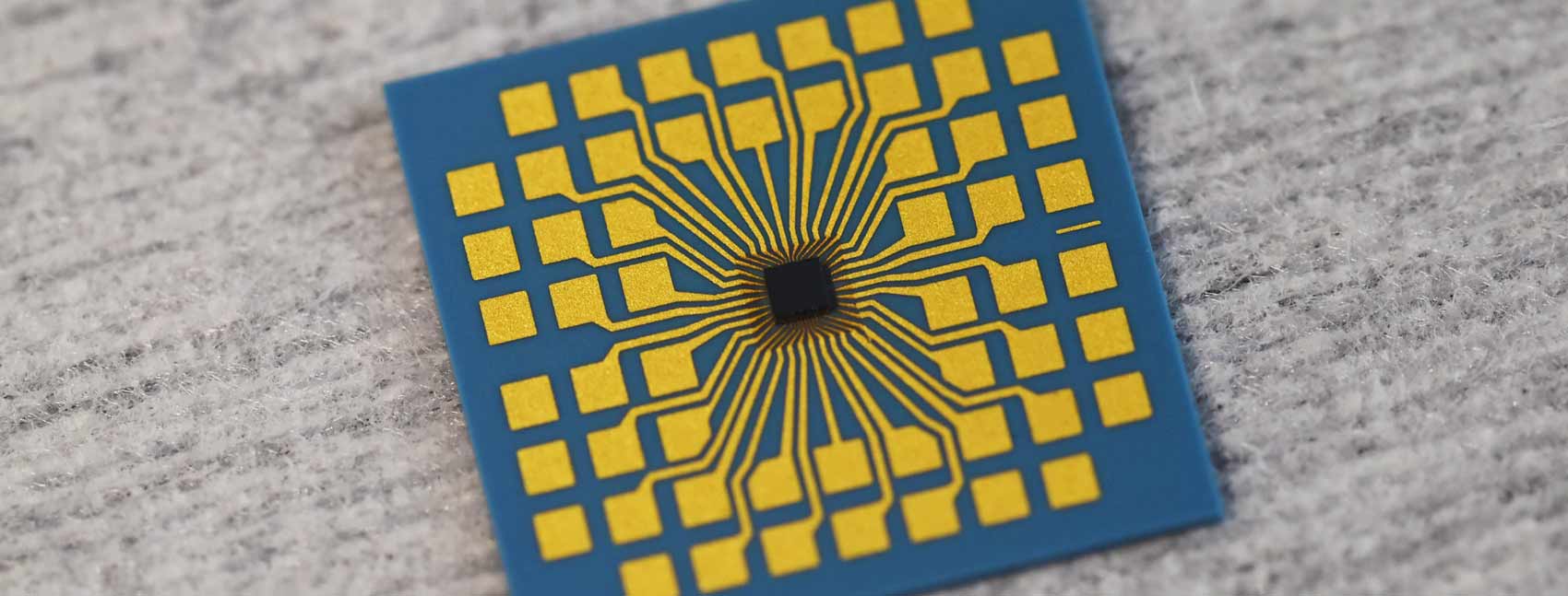
Circuits for high stress
Low Temperature Cofired Ceramics (LTCC) open up new fields of application as a substrate material compared to traditional printed circuit board materials. LTCC substrates enable multilayer electronic circuits to be used under harsh environmental conditions, such as high temperatures and pressures, contact with aggressive media, strong mechanical stresses or radiation exposure.
Fast prototyping
In cooperation with the Department of Electronics Technology and the Center for Micro- and Nanotechnologies we offer you the entire LTCC production line. This enables us to produce prototypes according to your requirements very flexibly and quickly.

Our production technologies
Based on the design, we provide screens with different emulsion thicknesses and screen cloths. In addition, the use of special fine-line screens is possible.
Vias and cavities for multilayer build-ups can be created both by means of high-precision punching technology (≥ 50 µm diameter) and by laser structuring using a UV picosecond laser (≥ 30 µm diameter).
The filling of the electrical vias is typically done by a bladder filling principle, but on customer request also with a stencil or screen.
We offer screen printing with different pastes, suitable for the different LTCC substrate materials. Fine line screen printing, laser structuring and lithographic structuring of films on different substrates offer the possibility of miniaturization.
The use of uniaxial and isostatic presses and special lamination aids allows the lamination of standard substrates as well as substrates with difficult topologies.
Sintering is performed in sintering furnaces with very uniform temperature profiles, either pressureless or pressure-supported.


