Miniaturized Circuits
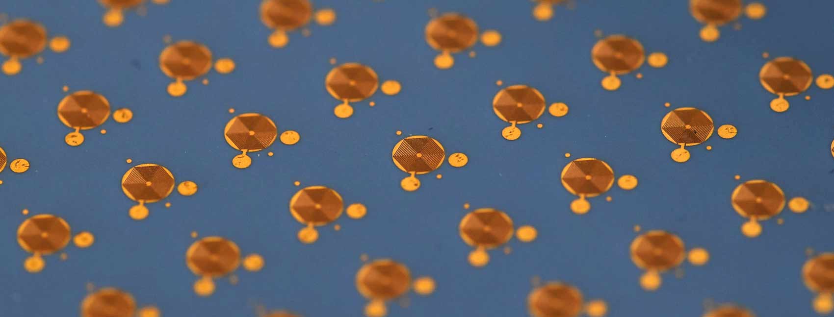
Laser structuring with a pulsed UV picosecond laser offers the advantage of processing with minimized thermal influence zones. The technologies we have developed enable the high-precision structuring of unfired, screen-printed thick films on LTCC green foils and the production of micro vias, as well as the structuring of layers on fired ceramic substrates, wafers or glasses. The structuring can be adapted quickly and flexibly to changed designs and fully integrated into the LTCC process chain.
With minimal structure dimensions down to 10 µm, a gap is closed between fine line screen printing, which is limited to a few materials, and complex lithographic structuring technologies.
At the same time, we can reduce the layer to layer offset of buried structures in multilayer structures down to 2.5 µm and smaller. Only this enables highly miniaturized circuits in LTCC.
High-precision laser structuring
Further fields of application of our picosecond laser structuring include thin-film structuring and the structuring of ceramics, glasses, metal foils and many other materials with very high demands on geometry and shape accuracy.
For the adaptation of printed thick film resistors we offer laser trimming processes based on the reduction of the cross section by cutting, but also the so-called laser shaping.